Trends in
Electronic Reliability -
Effects of Terrestrial Cosmic
Rays
J. F.
Ziegler
Trends
in SER of dRAM Memory Chips.
2
Trends
in SER of sRAM Memory Chips and Logic.
4
Flux
of Terrestrial Cosmic Rays. 6
Problems
in the Evaluation of Chip SER (Soft Error Rate)
7
Comments
on SER Modeling of chips. 7
Comments
on Accelerated Testing of chips.
7
Comments
on Life-Testing of Chips. 8
Introduction
This paper reviews the effects of cosmic rays on terrestrial electronics over the last twenty years. It will review separately the trends in soft-fail sensitivity of dRAMs, sRAMs and logic, and then show the difficult problems inherent in modeling and testing for chip sensitivity to terrestrial cosmic rays.
Over the last two decades, the sensitivity of electronics to radiation has been of increased interest as this mechanism dominates the soft-error rate (SER) of electronics- i. e. the spontaneous change of data or logic in systems. For terrestrial systems, two radiation mechanisms cause SER reliability problems: alpha-particles from radioactive contaminants in the chips, and cosmic rays. At terrestrial altitudes, more than 95% of cosmic rays are neutrons with fluxes below 1/cm2-min. Many memory chips are now sold with estimates of their alpha-particle SER, based mostly on the alpha particles fluxes from ceramic packages and lead-based connectors. These errors may be controlled by the use of purified materials, at additional cost. The SER from cosmic rays can be controlled by chip design, but adding robustness from design improvements is rarely done because of commercial pressures. This will be discussed below.
There are three synonymous terms used for the spontaneous changes of memory bits: “Soft Fails”, “Single Event Upsets”, SEU, and “Single Event Effects”, SEE. The first paper which evaluated upsets in satellites called the changes “anomalies”.[1] In 1978, Intel[2] reported that radioactive contamination on chips could cause changes in stored data, and used the term “soft fail”. This term is widely used in the commercial semiconductor industry. The first paper to predict the effects produced by cosmic rays (from IBM in 1979[3]) used “soft fails” to describe the events. Later the U.S. Naval Research Labs[4] demonstrated neutron radiation effects and coined the phrase SEU, single event upset, and this term is widely used by authors in space and military technology. Recently, the term SEE, single event effects, is replacing the use of SEU because of the observation of multiple-bit upsets. In general, all three terms are similar.
In 1996, a long review of the cosmic SER of electronic memories was published which listed over 300 citations of previously published works in this field.[5] Since that time, several experimental studies have evaluated the SER of more recent memory chips[6] - [7] [8] [9] [10] [11] [12] [13] [14] [15] [16] [17][18] [19], several theoretical studies have evaluated models for predicting SER[20] - [21] [22] [23] [24] [25] [26] [27] [28][29][30][31][32][33][34] [35], and various reviews have evaluated the SER of modern memory chips.[36] - [37] [38] [39] [40]
Trends in SER of dRAM Memory Chips
Originally, dRAM memory chips consisted of a single transistor with a bit-line controlling the source and a word-line controlling the gate. The device drain led directly to an adjacent capacitor consisting of a metal/ oxide layer over silicon. This capacitor’s charge indicated the stored bit. The capacitive charge induced in the substrate was slowly neutralized by charge migration in the silicon, and so the device information had to be renewed by stealing refresh cycles, hence the name “dynamic” RAM. After the introduction of 1Mb dRAM chips in 1989, there was no longer space to allow 4Mb on the chip, so manufacturers were forced to incorporate three-dimensional structures into their cell designs. By the introduction of 16Mb memory chips, three different approaches to cell technology for storing the bit charge had been adopted: the stacked capacitor with high-dielectric layers, a trench with the stored charge insulated from the substrate, and a trench with the charge stored using a p/n junction isolation from the substrate material. See Figure 1.
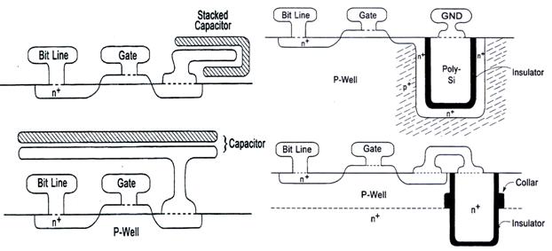
Figure 1
dRAM Designs
Modern dRAM chips use various 3-D concepts to build the capacitor which holds the electronic bit information. The left schematics show two forms of “stacked capacitor” designs in which the capacitor is formed above the device using one or more contact layers (only one is shown in the diagram).The two schematics on the right are based on trench technology in which deep trenches are etched into the silicon (the depth:width may be 10:1). In the upper-right design the trench contains an insulating layer with an inner metallic contact. The silicon substrate holds the opposing charge and thus this design is similar to the original dRAM concept. The lower-right design includes a trench which contains both plates of the capacitor. (from Ref. 13)
The sensitivity of dRAMs to radiation has dramatically improved over the last 15 years, see Figure 2. This improvement has been attributed to the significant reduction in dRAM volume per cell, and also the lack of commercial pressure to increase cell speed. The reduction of the active volume of dRAMs is unique with this CMOS device since the newer cell designs shown in Figure 1 eliminate funneling of charge from the substrate (to be discussed later concerning sRAMs). The commercial pressure on dRAM chips has always been to increase the bits per chip and not their speed. This has allowed some engineering effort to be devoted to reliability. Since almost no PCs and only some mid-frames have error detection on their memories, electronic reliability in dRAMs is important.
The data shown in Figure 2 are results for traditional dRAM designs through the 1 Mb chips, and then switches to the 3-D design shown in the lower-right of Figure 1, “Trench. Internal-Charge”. This design has no charge stored in the silicon substrate so that there is little leakage – storage times for cell charge retention has been reported to be tens of milliseconds.
There are about 16 manufacturers of dRAM chips, and all have been tested for sensitivity to cosmic ray neutrons. Their sensitivities are shown in Figure 3.
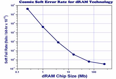
Figure 2 The change of dRAM chip sensitivity to
cosmic rays over 15 years
The soft error rate per bit has dropped by six orders of magnitude over this period. The plot shows the fail rate / bit-hr. For a 32MB memory, if it was populated by 256 kb chips (circa 1985) shown above, the fail rate would be about once every eight hours. If it was populated by 256 Mb chips, the next century may pass without an error. (from Ref. 5)
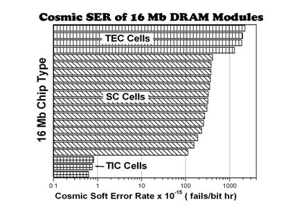
Figure 3 Soft Error Rate of 16Mb
Memories
The Soft Error Rate of 21 different 16Mb chips from nine vendors shows more than 1000x variation. The SER sensitivity is directly related to the dRAM design as described in Figure 1. The Trench External-Charge (TEC) designs are very sensitive because charge is stored in the silicon substrate which greatly expands the active volume of the cell. The Stacked Capacitor (SC) cells all have similar sensitivity. The Trench Internal-Charge (TIC) cells are very robust, showing little sensitivity to cosmic rays.(from Ref. 13)
Trends in SER of sRAM Memory Chips and Logic
The soft error rate (SER) of sRAM chips is simpler than dRAMs to evaluate since there have been no attempts at 3-D structures such as occurred in dRAMs. Most CMOS based sRAMS are similar. The only radical technology introduced has been the use of Silicon-on-Insulator (SOI), adopted by IBM in 1998 and slowly spreading throughout the semiconductor industry for high performance applications.
sRAMs have bit cells made in two different ways: with four or six device cells forming each bit flip-flop. The four device cell uses two resistive layers to couple the flip-flop devices, while the six device cell replaces these two resistors with passive devices.
The introduction of SOI would be expected to have significant impact on the SER of bipolar transistors, and also the TEC dRAM cells described previously. Both of these have active layers immersed in the silicon substrate and would be sensitive to charge bursts deep in the silicon. However, in the current decade, both of these technologies are used only for niche products and are not mainstream for digital applications. The effect of transplanting a microprocessor or sRAM chip to SOI should have limited impact on cosmic ray reliability. Estimates usually are of the order of 3x reduction, or less. No experimental SER data has been presented by any of the manufacturers of SOI chips.
The trend in the sensitivity of sRAM and logic to cosmic rays is shown in Figure 4.
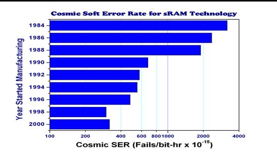
Figure 4 Trends in sRAM cosmic ray SER,
1984-2000
The SER of sRAMs is plotted for devices from 1984-2000. The upper three bars, 1984-1988, are for bipolar sRAM chips, while the later ones are CMOS based. The change from bipolar to CMOS made an immediate improvement in SER because of the well structure of CMOS devices, preventing charge from deep in the substrate from reaching active device elements. The total fail rate per bit over 16 years has dropped about 10x, but during the same period the bits per chip has increased about 1000x. (from Ref. [41])
The details of the sensitivity of sRAM chips to neutrons have undergone remarkable changes over time. See Figure 5, which shows the fail rate of CMOS sRAM chips vs. neutron energy since 1988 as determined by accelerated testing (exposing chips to nucleon beams are various energies).
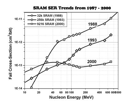
Figure 5 The SER of
CMOS sRAM chips from 1988 to 1999 as a function of nucleon
energy.
The 1988 chips shows a 1000x increase in SER fail rate from 10 Mev to 1000 MeV nucleons. Over the next decade, sRAM circuits became more sensitive to lower energy particles and almost 100x less sensitive to high energy particles. Modelers have ascribed the high energy drop to a decrease in active volume of the devices. The increase in sensitivity to low energy neutrons has not been explained. (from Ref. 41)
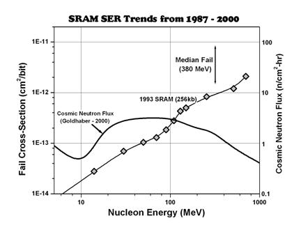
Figure 6
Combining chip fail cross-section with cosmic flux to obtain chip
SER
A chip’s fail rate vs. nucleon energy can be combined with the terrestrial flux of nucleons vs. energy to determine the chip SER. Above is a typical 1993 sRAM fail rate along with the sea level flux of neutrons as recently determined by Goldhaber. The SER is the area under the product of these two curves. For the above example, the median particle-energy for a memory fail would be for a nucleon of about 380 MeV. (from Ref. 41)
A prediction of the fail rate of a memory chip at terrestrial altitudes may be determined by integrating the chip fail rate vs. nucleon energy (Figure 5) with the flux of nucleons at a location such as Goldhaber-2000 shown in Figure 6:
SER = ò
(Fail cross-section
[fails/(nucleon/cm2)])(Flux of nucleons
[nucleons/cm2-hour])
= Fails / hour
The flux of nucleons will vary depending mostly on the site altitude (up to 10x) and solar cycle (up to 30%). Since at terrestrial altitudes the nucleon flux is >96% neutrons, these are the only particles usually considered in calculations of SER.
Flux of Terrestrial Cosmic Rays
The last section described the calculation of the terrestrial SER of chips based upon their fail rate using particle beams combined with the terrestrial flux of neutrons. The flux of particles at sea level has been reported by ten authors, mostly as initial calibration values for balloon or air flights. Shown in Figure 7 is a summary these results over the region of interest for SER evaluation.
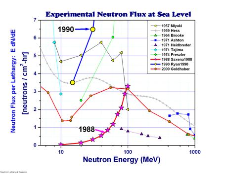
Figure 7 – Experimental results of cosmic ray
neutrons at sea level.
Experimental measurements of the flux of cosmic ray neutrons are shown from ten papers. The plot shows that there is no consensus of the actual flux. The values marked “1988” and “1990” were from a three year research study commissioned by IBM. The values of Saxena (a PhD student) were the “final” values reported (see data marked 1988). This same data was reanalyzed by Professor Ryan and resulted in the values, 1990, which reached intensities up to 20 neutrons/cm2-hr. (from Ref. [42])
The results shown in Figure 7 indicate the lack of agreement about the terrestrial flux of neutrons. If the fail cross-sections shown in Figure 5 are used to calculate chip SER, assuming the recent Goldhaber flux values, one can determine the median energy for chip fails. These energies are shown in the Table below:
|
CMOS sRAM Chip Mfg. Year |
Median Neutron Energy of Fails |
|
1988 |
900 MeV |
|
1993 |
380 MeV |
|
2000 |
80 MeV |
The change in SER cross-section between 1988-2000 (see Figure 5) has had a dramatic affect on the median neutron energy for SER. Since modern chips, post-2000, have a median fail from neutrons below 100 MeV, the wide variation in flux measurements limits the accuracy of predicting chip SER. Below 100 MeV, the cosmic neutron flux is due to the last collisions of the cosmic ray cascade. For most buildings, this cascade will probably initiate in the building walls. There have been no papers which tried to address this last cascade, and how it effects the cosmic neutron flux within buildings.
Problems in the Evaluation of Chip SER (Soft Error Rate)
The SER of chips can be evaluated from four complementary methods:
·
Modeling.
·
Accelerated testing.
·
Life testing.
·
Field reports of
reliability.
The most important evaluation is from device modeling, since this SER evaluation allows an engineer to focus on weak-links in the circuit and device design at the earliest stages of development. Most chips with anomalously high SER have been shown to suffer from weak-links, i. e. single components which were included without consideration of their SER contribution. Examples would be floating bit-lines, insufficient margins on sense-amplifiers and junctions exposed to the silicon substrate.
Accelerated testing, i.e. exposing the chip to various types of radiation, can be done as soon as chips are available, and at small cost. However, chips must already have progressed to the manufacturing stage to allow accurate measurements. This severely limits the amount of redesign that can be done the on the chip and makes SER evaluations only possible in the final stages of chip development.
Life-testing is the evaluation of chip SER by using a tester containing hundreds of chips and evaluating their fail rate under nominal conditions. Life testing is the most accurate way to determine SER, but it is very expensive, and make take up to a year after manufacturing begins to obtain reliable results. Except for fire-fights, it is relatively useless to industry since the chip is moving towards obsolescence before SER results are known.
Field reports of reliability - The worst possible method of determining chip SER is from screaming field customers, but often this is the trigger required for SER studies.
Comments on SER
Modeling of
chips
As of 2002, there are no comprehensive models available to predict the SER of sRAMs or dRAMs. None of the existing modeling programs include adequate low-energy neutron cross-sections which would allow the SER prediction of circuits within a factor of 2x. Also, there are no reliable estimates of the flux of low-energy particles. Current measurements vary up to 100x, possibly due to the influence of local building materials on the flux, which has not been previously been considered. Without knowledge of the flux of particles, no model can predict a chip's SER.
Comments on Accelerated Testing of chips
The accelerated testing of chips is done by the irradiation of chips with various hadrons (hadron = particles which have the strong-interaction, also called the nuclear force). The primary hadrons for SER testing are protons, neutrons, alpha particles and pions. Pions are of limited concern at terrestrial altitudes, but may be important at aircraft altitudes. The flux of protons at sealevel is less than 3% of the total, so the SER of chips can be estimated by just considering neutron interactions. However, it has been shown that protons above 30 MeV have almost identical SER cross-sections as neutrons, since above this energy the charge on the proton has negligible effect on nuclear cross-sections. And since proton beams are more readily available, SER testing usually involves using neutron beams for energies below 30 MeV, and protons above this energy.
Comments on Life-Testing of Chips
Life-testing is the evaluation of chip SER by using a tester containing hundreds of chips and evaluating their fail rate under nominal conditions. The life testing of chips is both slow and very very expensive (typically about $300k/chip). However, it is required to validate modeling and accelerated testing.
Difficulties of Life Testing at Nominal Voltages
Life testing at nominal conditions is
very frustrating. For example, assume a tester which holds 500 chips which have
an estimated SER of about 5000x10-9 fails/hr. This is a typical
modern SRAM fail rate per chip. In order to get 50% reliability at
two-sigma, you will need to wait for 16 fails or about 9 months. This means that
the SER results will not be available until about a year after the first chips
start coming out of the fabrication line.
This long delay is generally unacceptable. The alternative is either the costly path of testing many more chips with a bigger tester, or to deviate from the nominal conditions and test the chips in a more sensitive state, i. e. at reduced voltage.
Difficulties of Life Testing at Reduced Voltages
Chips become much more sensitive to radiation at reduced voltages. Often, a factor of 10x increase in sensitivity may be obtained by operating the chip just above its voltage of instability. However, this low-voltage testing has a serious problem, illustrated in Figure 8.
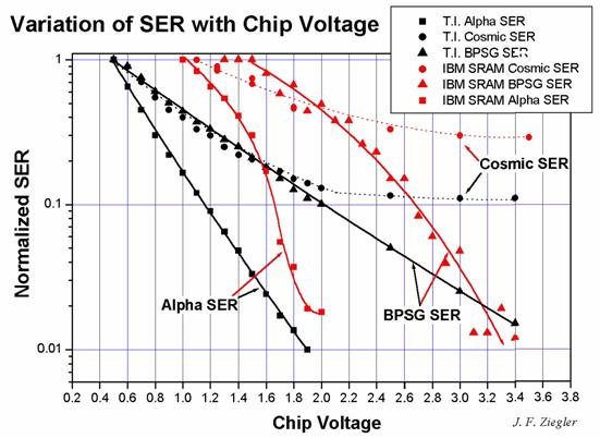
Figure 8 – SER Sensitivity of SRAMs with Reduced
Voltage.
The plot shows how two SRAM chips vary in SER sensitivity at reduced voltage (a typical SRAM from TI, and one from IBM). The data has been broken into three components based on chip testing using different types of particles. The sensitivity to alpha-particles has the most dramatic change with voltage, with 10x changes over less than ½ volt. The chip sensitivity to thermal neutrons (indicated by the label “BPSG SER”) is intermediate in slope. The chip sensitivity to high energy neutrons, > 1 MeV, has the least SER change with bias.
Figure 8 shows that various components of chip SER have significantly different sensitivity to changes in chip bias. If chips under life-test are operated at reduced voltage in order to increase their sensitivity to radiation, the different types of particles will have very different changes in their contributions to the overall SER. From the data presented in Figure 8 one can see that both TI and IBM sRAMs will greatly increase their sensitivity to radiation by decreasing their operating voltage. However, most of the increased sensitivity will be due to the SER of alpha particles and less change will be due to cosmic ray fails (particles with energies > 1 MeV). The alpha particle SER component may be isolated by life-testing chips underground, eliminating the cosmic ray SER component. But is a this further burden on the time and cost of life testing.[43]
The purpose of life-testing is to evaluate the chip SER under nominal conditions. So if the testing is done at reduced voltages, one must scale the test results at reduced bias back the nominal chip voltage. This may only be done if one has evaluated the individual chip sensitivity vs. voltage to each of the components of its SER. Hence, the data contained in Figure 8 must be obtained in order to convert the life-test values obtained at reduced voltage back to the chip’s nominal conditions. Even then, the results are of dubious value, for one must assume the contribution of each component of the chip SER, e. g. that alpha particles cause 20% of the fails, etc. If any of the assumptions about the magnitude of each component is wrong, then the final estimated chip SER will be in error.
Conclusions
·
dRAM
sensitivity to cosmic rays has dropped about six orders of magnitude over 15
years, on a per bit basis. This can be attributed to the decreased active volume
and lack of commercial pressure to increase access speed. However, 16Mb dRAM
chip SER from different manufacturers differs by more than
1000x.
·
High
performance sRAM sensitivity to cosmic rays has dropped about 10x over the last
15 years, while the bits/chip has increased 1000x. Hence the net fail rate per
chip has increased about 100x.
·
Modern
CMOS chips are mostly sensitive to neutrons below 100 MeV. There are no reliable
estimates of the cosmic neutron flux at these energies.
·
Modeling of chip SER is not available because of the
lack of realistic models and the unreliability of the cosmic flux at energies of
interest.
·
Accelerated Testing of chip SER is unreliable because of lack
of knowledge of the terrestrial cosmic flux at energies of
interest.
·
Life
Testing might be useful to validate Accelerated Testing or Modeling, but it is not useful to
evaluate actual chips. Full voltage testing is expensive and takes so long that
its results are rarely useful. Reduced voltage (enhanced sensitivity) testing
has too many pitfalls and assumptions to be used with confidence.